
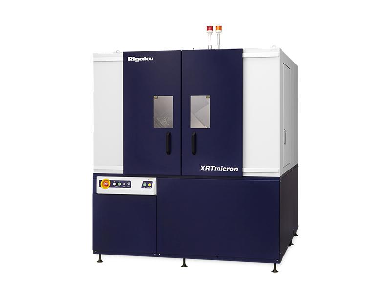
XRTmicron
X-RAY TOPOGRAPHY IMAGING SYSTEM
For non-destructive evaluation of single-crystalline materials
Features
- High-brilliance dual-wavelength X-ray source: MicroMax-007 DW
- High resolution CCD camera: XTOP (5.4 μm pixels)
- Ultra-high resolution CCD camera: HR-XTOP (2.4 μm pixels)
- Horizontal sample mount for minimum artificial strain to wafers
- Automatic wafer curvature correction for best dislocation image quality
- Automated system operation including X-ray anode switch, detector switch, optics switch and alignment, sample alignment, and image collection
- Automated dislocation analysis
- 3, 4, 6, 8, 12 inch wafers supported
- Wafer loader compatible
NON-DESTRUCTIVE DISLOCATION IMAGING
Rigaku XRTmicron is a non-destructive dislocation imaging system with a quick, high-resolution laboratory X-ray topography system. Various sorts of dislocations and non-uniformity can be photographed across wafers up to 300 mm in diameter in single crystal wafers (such as Si, SiC, GaN, Ge, GaAs, quartz, sapphire, rutile, calcium fluoride, and so on). X-ray topography is a widely utilised dislocation analysis technique by single crystal, wafer, and device makers for both research and development and process control.
TOPOGRAPHY ENGINEERED FOR PERFORMANCE
Combining a high-brilliance dual-wavelengths X-ray source, the MicroMax-007 DW, and X-ray mirrors designed for the topographical application, the MicroMax-007 DW achieves unmatched scan speed 10 times faster than standard systems. Cu and Mo X-ray anodes, as well as their mirrors, are installed on the system simultaneously and swapped on-demand to perform reflection and transmission measurements without requiring any system reconfiguration. A high resolution (5.4 m pixels) or ultra-high resolution (2.4 m pixels) CCD camera captures a digital image of dislocations. Both cameras can be put on the system at the same time and swapped on-demand depending on the resolution necessary.
FULLY AUTOMATED X-RAY TOPOGRAPHY
Engineered for usability, the entire data image collection process – including anode switch, detector switch, optics switch and alignment, sample alignment and image collection – is fully automated. Furthermore, the system can be combined with a wafer loader and image recognition based dislocation counting software. Customized recipes can be built to automate the entire process from loading a wafer to reporting dislocation densities.
Specifications Table
| Product name | XRTmicron |
| Technique | X-ray topography |
| Benefit | Non-destructive evaluation of single-crystalline materials |
| Technology | Imaging using X-rays |
| Core attributes | High-flux multi-target X-ray source, CCD imager |
| Core options | XTOP or HR-XTOP CCD |
| Computer | External PC, MS Windows® OS, |
| Core dimensions | 1800 (W) x 1800 (H) x 1870 (D) (mm) |
| Mass (core unit) | 2200 kg |
| Power requirements | 3Ø, 200 V, 15 A |